rajkot

Saturday, July 16, 2011

TELEPHONE OPERATED REMOTE

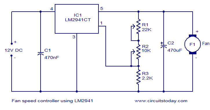
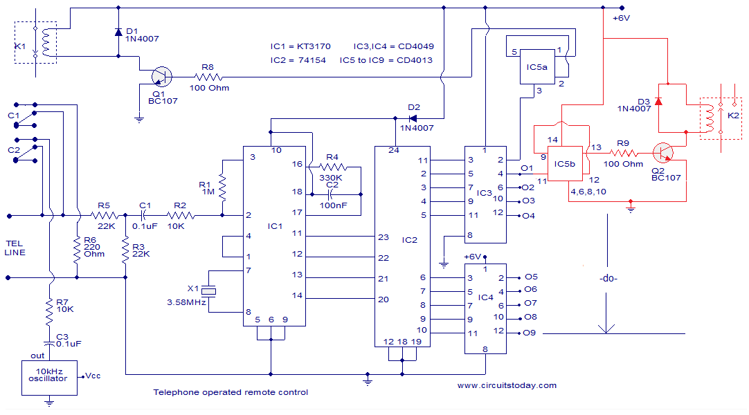
  1. The circuit given below is of a telephone operated DTMF remote. The circuit can be used to switch up to 9 devices using the keys 0 to 9 of the telephone. Digit 0 is used to switch the telephone system between remote switching mode and normal conversation mode.
  2. IC KT3170 (DTMF to BCD decoder) is used to decode the DTMF signals transmitted over the telephone line to corresponding BCD format. IC 74154 ( 4 to 16 demultiplexer) and IC CD4023 (dual D flip flop) is used to switch the device according to the receive DTMF signal.
  3. The operation of the circuit is as follows. After hearing the ringtone from the phone at receiver end, press the 0 button of the remote phone. 
  4. The IC1 will decode this as 1010.The pin 11 of IC2 will go low and after inversion by the NOT gate in IC3 it will be high. This will toggle the flip flop IC5a and the transistor Q1 will be switched on. This will make the relay K1 ON. The two contacts C1 and C2 of the relay K1 will be closed.
  5. C1 will form a 220 Ohm loop across the telephone line in order to disconnect the ringer from the telephone line (this condition is similar to taking the telephone receiver off hook).C2 will connect a 10KHz audio source to the telephone line in order to inform you that the system is now in the remote switch mode.
  6. Now if you press 1 on the transmitter phone, the IC1 will decode it as 0001 and the pin 2 of IC2 will go low. After inversion by the corresponding NOT gate inside IC3, it will be high. This will toggle flip flop IC5b and transistor Q2 will be switched ON. The relay will be energized and the device connected through its contacts gets switched. 
  7. Pressing the 1 again will toggle the state of device. In the same ways Keys 2 to 9 on the transmitter phone can be used to toggle the state of the device connected to the channels O2 to O9. After switching is over, press the O key on the transmitter phone in order to toggle the flip flop IC5a to de-energize the relay K1.The 200 Ohm loop will be disconnected from the line, the 10 KHz audio source will be removed and the telephone receiver will be ready to receive new calls.


NOTES:
  • Assemble the circuit on a good quality PCB.
  • Use 6V DC for powering the circuit.
  • A simple NE555 based oscillator can be used as the 10 KHz audio source.
  • All IC’s must be mounted on holders.
  • The section drawn in red must be repeated eight times (not shown in circuit).
  • In certain countries circuits like this cannot be connected to telephone line.I do not have any responsibility on the legal issues .

Tuesday, June 28, 2011

LED BASED TRANSISTOR TESTER

  1. Here is the circuit of a very simple transistor tester which used two LEDs for displaying the condition of a transistor. Both PNP as well as NPN transistors can be tested using this circuit. 
  2. Quad 2 input CMOS NAND gate IC CD4011B is the heart of the circuit. Out of the four NAND gates inside the IC, only three are used here and they are used as NOT gates by shorting their input terminals.
  3. Gates U1a, U1b, resistor R1 and capacitor C1 forms a square wave oscillator. The frequency of this oscillator can be adjusted by using R1. The output of the oscillator is inverted using the gate U1c. 
  4. The inverted oscillator output is connected to the base of the transistor under test through the resistor R2 and the non inverted oscillator output is connected to the emitter of the transistor under test using the resistor R3.
  5. The status of the LEDs D1 and D2 reveals the condition of the transistor under test. If red LED is ON, It indicates that the transistor under test is a good NPN. 
  6. If green LED is ON, it indicates that the transistor under test is a good PNP. If both LEDs are ON, it indicates that the transistor under test is short.
  7. If both LEDs are OFF, it indicates that either the transistor is bad or you may have connected it incorrectly.


NOTES:
  • The circuit can be easily assembled on a Vero board.
  • Use 5V DC for powering the circuit.
  • All unused pins of the IC must be connected to ground.

Monday, April 18, 2011

TV ANTENNA BOOSTER

  1. The circuit shown here is of a TV antenna booster based on the transistor BF180. The circuit operates in the UHF band and has a gain of 15dB.
  2. Capacitors C2,C3 C4 ,C5 and inductors L3, L4 forms a UHF band pass filter. The input signal is fed to the emitter of Q1 through this filter.
  3. Resistor R2 and R3 biases the transistor Q1 which is wired in the common base configuration.


NOTES:
  • Assemble the circuit on a good quality PCB.
  • For better performance, enclose the circuit in a metal box.
  • The circuit can be powered from 12V DC.

Saturday, April 16, 2011

SCORING GAME CIRCUIT

  1. A simple scoring game circuit that can be used for all occasions when a dice is needed.The circuit is based on a NE555 timer,a 74LS192 counter,a74LS247 decoder and a & segment LED display.
  2. The timer IC1 will produce the clock for the counter IC(IC2) whose frequency is determined by R1 and C2.When S2 is pressed the IC2 will count in up mode and when S3 is pressed the IC2 will count in down mode.The IC 3 will decode the count to display it on the seven segment LED display .Thats about the working of the circuit.The circuit is designed strictly sticking on to the basics of counters and is a good one for beginners.


     NOTES:
  • To play the game switch the power ON and press S1 to reset the counter.
  • Now press S2 or S3 and release .The IC2 will hold the last count .Now press S4 to see the score on display.That’s your score.Now the second person can try.
  • Each time one tries, he should press the S1 to reset the count and then press S2 or S3 and then S4 to see the score.
  • Circuit can be powered from a 9V radio cell or a 9V regulated DC power supply .

Thursday, February 17, 2011

STEREO FM TRANSMITTR CIRCUIT USING BA1404

  1. A high quality stereo FM transmitter circuit is shown here. The circuit is based on the IC BA1404 from ROHM Semiconductors.
  2. BA1404 is a monolithic FM stereo modulator that has built in stereo modulator, FM modulator, RF amplifier circuitries. The FM modulator can be operated from 76 to 108MHz and power supply for the circuit can be anything between 1.25 to 3 volts.
  3. In the circuit R7, C16, C14 and R6, C15, C13 forms the pre-emphasis network for the right and left channels respectively.
  4. This is done for matching the frequency response of the FM transmitter with the FM receiver. Inductor L1 and capacitor C5 is used to set the oscillator frequency.
  5. Network C9,C10, R4,R5 improves the channel separation. 38kHz crystal X1 is connected between pins 5 and 6 of the IC. 
  6. Composite stereo signal is created by the stereo modulator circuit using the 38kHz quartz controlled frequency.


    NOTES:
    • Assemble the circuit on a good quality PCB.
    • Powering the circuit from a battery will reduce noise.
    • Use an 80 cm copper wire as antenna.
    • For L1 make 3 turns of 0.5mm dia enamelled copper wire on a 5mm dia ferrite core.

Tuesday, February 15, 2011

BUCK BOOST CONVERTER CIRCUIT

  1. A very efficient buck boost converter circuit is shown here. The circuit is based on the LTC3440 buck boost regulator IC from Linear Technology.
  2. The LTC3440 requires only one inductor and provides up to 96% efficiency. There is no need of Schottky diode for applications where output voltage is less than 4.3V and the IC can deliver up to 600mA output current.
  3. In the circuit the IC is wired as a buck boost regulator providing 3.3V output from a 2.7 to 4.2V input.
  4. R1 is the timing resistor which determines the oscillator frequency and it can be varied between 300 KHz to 2MHz by varying the value of R1. C1 is the input bypass capacitor for reducing noise and C3 is the output filter capacitor.
  5. Resistors R4, R4 sets the output voltage and the network consisting of C2 and R2 is meant for frequency compensation.


    NOTES:
    • Assemble the circuit on a good quality PCB.
    • Input voltage can be between 2.7 to 4.2V.
    • L1 can be a toroid, potcore or shielded bobbin inductor.
    • C1 to C3 are ceramic capacitors.

Thursday, February 3, 2011

AM RECEIVER USING ZM 414Z

  1. This is the circuit diagram of the simplest single chip AM radio
  2. The circuit is designed around the IC ZN414Z which is a ten transistor tuned radio frequency receiver .The IC has only three leads and is available in the TO92 package.
  3. All necessary circuits required for an AM receiver (RF amplifier, detector and AGC are incorporated inside the IC).
  4. Capacitor C4 decouples DC from the output of the IC and C1 bye-passes the noise.
  5. Transistor Q1 and associated components forms a classic driver stage for the headphone.
  6. Head phone is connected across the resistor R5 and R4 gives necessary biasing for the transistor Q1.


    NOTES:
    • Assemble the circuit on a good quality PCB.
    • The circuit can be powered from a 1.5V cell.
    • Do not give more than 1.8V to the circuit as it will destroy the IC.
    • For L1 make 80 turns of 0.3mm enameled copper wire on a 5cm long ferrite rod.
    • K1 can be a high impedance crystal earpiece.

Wednesday, February 2, 2011

AUTOMOBILE TURN SIGNAL CIRCUIT

 
  1. This is a simple circuit that can be used as a sequencial signal light in automobiles.
  2. The circuit is based on two ICs. A TS 555 CN CMOS timer IC and a CD4017 decade counter IC
  3. The IC1 is wired as an astable multivibrator to trigger the counter IC. When triggered, the outputs of the IC 2 (pins 3, 2, 4 and 7) will go high and low in sequence and the speed of this sequencing will be proportional to the triggering frequency.
  4. The transistors Q1 to Q4 drives the corresponding LEDs.
  5. The switch S1 can be used to select the direction of turning and the LEDs arranged at the corresponding side of vehicle will start sequencing.
     NOTES:
    • The switch S1 can be the existing changeover switch of the vehicle it self.
    • The circuit can be powered of the 12V available from the vehicle itself.
    • The color of the LED depends on your choice .
    • The ICs must be mounted on IC holders.
    • Assemble the circuit on a good quality PCB .
    • Be careful with the wiring of this circuit because any wrong connection may put the electricals of your vehicle  in trouble.


Tuesday, February 1, 2011

FAN SPEED CONTROLLER USING LM2941

  1. Many electronic circuits related to fan speed controlling have been published here and this one is just another approach. 
  2. The circuit diagram shown here is of 12V DC fan speed controller using the IC LM2941CT which is a low drop out 1A voltage regulator. The IC has a dropout voltage as low as 0.5 and has also many useful features like power supply reverse protection, thermal protection, short circuit protection etc.
  3. The maximum output current the IC can source is 1A.
  4. The 12V DC supply is connected between the Vin (pin4) and ground (pin3) of the IC.
  5.  The load, which is the fan, is connected across the Vout (pin5) and ground (pin3) of the IC. The network comprising of potentiometers R1, R2 and resistor determines adjust current (Iadj) of the IC.
  6. By varying the Iadj using the POT R2 we can adjust the output voltage of the IC and hence the fan speed.
    NOTES:
    • The circuit can be powered from 12V DC.
    • The maximum possible load current is 1A.
    • A heat sink is recommended for the IC.
    • POT R1 can be used to adjust the minimum fan speed.
    • POT R2 can be used to adjust the fan speed.


Sunday, October 3, 2010

TWEETER CROSSOVER CIRCUIT

  1. A single coil speaker is not good in handling high and low frequency at the same time.
  2. If we could filter out the low frequency and play it through a tweeter ,it will produce more sound quality than using a single speaker.
  3.  This is what is realized here.
  4.  Here the high frequencies are filtered out using a low pass filter made of C1,C2 and R1 and send to the tweeter.The low frequency is only fed to the woofer.
    NOTES:
    • The tweeter can be a 2 to 3 inch, 4 to 8 Ohm one .
    •  R1 is used to adjust match the the tweeters output level to that of woofer.
    • C1 and C2 are electrolytic capacitors.
    • R1 should be rated more than 2 Watts.

Monday, September 20, 2010

LED TOURCH USING MAX 660

  1. This is a simple LED torch circuit based on IC MAX660 from MAXIM semiconductors.
  2. The MAX 660 is a CMOS type monolithic type voltage converter IC. 
  3. The IC can easily drive three extra bright white LEDs.The LEDs are connected in parallel to the output pin 8 of the IC.
  4. The circuit has good battery life. The switch S1 can be a push to ON switch.

    NOTES:-
    • Assemble the circuit on a general purpose PCB.
    • The IC must be mounted on a holder.
    • The circuit can be powered from two torch cells connected in series.
    • The capacitors C1 and C2 must be Tantalum type.
    • The diodes D1 to D3 must be of 1N4148.

Wednesday, September 15, 2010

CW PRACTICE OSILLATOR

    1. A circuit diagram that can be used for the generation of CW Morse code is shown here.
    2.  This circuit can be very useful those who would like practice Ham Radio.
    3.  The circuit is nothing but an astable multivibrator based on NE 555.The frequency of oscillations of the circuit depends on the components R1,R2 & C1.The circuit can be powered from a 9V PP3 battery. .


    NOTES:
    • The POT R2 can be used for frequency adjustments.
    • POT R3 can be used for volume adjustments.
    • The switch S1 can  be a Morse code key.

Monday, September 6, 2010

10V SWITCHING REGULATOR USING LM5007

  1. The circuit diagram shown here is of a 10V switching regulator based on the LM5007 from National Semiconductors.
  2. The LM5007 is an integrated step down switching regulator which has all necessary systems required for making a cost effective and reliable switching regulator circuit.
  3. The IC is available in MSOP-8, LLp-8 packages and has a lot of  built in  features like thermal shut down, under voltage lock out, duty cycle limiting, current limiting etc.
  4. The output voltage of this regulator can be adjusted using the resistor R3 and R4. 
  5. OR the given values of R3 and R4 in the circuit diagram, the output voltage will be 10V.
  6. he equation governing the output voltage is Vout = 2.5 x (R3+R4)/R4. Resistor R1 sets the switch on time and C4 is the boost boot strap capacitor.
  7. Resistor R2 determines the variation of OFF time and C3 is a decoupling capacitor.


    NOTES:
  • The supply voltage can be anything between 12 to 72V DC.
  • Output voltage can be adjusted using R3 and R4.
  • C1  and C5 are polyester capacitors.
  • C1 and C2 must be rated at least 100V.
  • R5 and C5 forms a filter network.
  • The output current limit of LM5007 is 700mA.

Tuesday, August 17, 2010

3 INPUT MICROPHONE PREAMPLIFIRE

  1. The circuit given here is of a three input mic mixer cum preamplifier using the IC LM348. The LM348 is a high gain, internally compensated quad operational amplifier with a class AB output stage.
  2. The IC has very low input supply current drain (0.6mA/ opamp) and operates from a dual power supply.
  3. Out of the four op-amps inside the IC LM348, IC1a, IC1b and IC1c are wired as non inverting amplifiers and they serve as the input amplifiers for the corresponding mic channels. 
  4. The output of these three amplifiers are tied together and connected to the inverting input of the IC1a which is wired as an inverting amplifier.IC1a mixes the signals from each channel and also works as the output stage.


    NOTES:
    • Assemble the circuit on a good quality PCB.
    • Use +12/-12V DC dual supply for powering the circuit.
    • The power supply must be well regulated and filtered.
    • POT R5 to R7 can b e used for adjusting the gain of individual channels.


Tuesday, August 10, 2010

STEREO PREAMPLIFIER WITH TONE CONTROL

  1. Here is the circuit diagram of an excellent stereo preamplifier with tone control using the IC TDA1524 from Phillips.
  2. The IC requires very few external components, has very low noise and has a wide power supply voltage range.
  3. POTs R1 to R4 can be used for controlling the volume, balance, bass and treble respectively.

  4. LED is D1 is a power ON indicator and R1o is its current limiting resistor.


    NOTES:
    • Assemble the circuit on a good quality PCB.
    • Switch S2 is the ON/OFF switch.
    • Swich S1 can be used to select linear or contour mode.
    • Supply voltage can be anything between 8 to 16V .Here I used 12V DC.


Wednesday, August 4, 2010

DARK DETECTOR

  1. The dark detector circuit shown here can be used to produce an audible alarm when the light inside a room goes OFF.
  2. The circuit is build around timer IC NE555.A general purpose LDR is used for sensing the light. 
  3.  When proper light is falling on the LDR its resistance is very low.
  4. When there is no light the LDR resistance increases.
  5.   At this time the IC is triggered and drives the buzzer to produce an alarm sound.
  6.  If a transistor and relay is connected at the output (pin3) of IC1 instead of the buzzer, electrical appliances can be switched according to the light.


    NOTES:
    • The LDR ,R4 can be any general purpose LDR.
    • The circuit must be assembled on  a good quality PCB or  common board.
    • The circuit can be powered from a 9V PP3 battery.
    • The POT,R3 can be sued as a volume controller.
    • Mount the IC1 on a holder.It will make replacements easy.

Tuesday, August 3, 2010

PARKING SENSOR CIRCUIT

  1. This simple circuit can be used as an aid for sensing the distance between the rear bumper of the car and any obstacle behind the car. The distance can be understood from the combination of the LEDs (D5 to D7) glowing. At 25cm D7 will glow, at 20 cm D7&D6 will glow and at 5cm D7, D6 and D5 will glow. When the obstacle is beyond 25 cm none of the above LEDs will glow.
  2.  Two ICs are used in the circuit. The IC1 (NE555) is wired as an astable multivibrator for driving the IR Diode D1 to emit IR pulses. The operating frequency of the transmitter is set to be 120Hz.
  3.  The IR pulses transmitted by D1 will be reflected by the obstacle and received by the D2 (IR photo diode).The received signal will be amplified by IC2a.The peak of the amplified signal will be detected by the diode D4 and capacitor C4.R5 and R6 compensates the forward voltage drop of D4.The output voltage of the peak detector will be proportional to the distance between car’s bumper and obstacle.
  4. The output of peak detector is given to the inputs of the other three comparators IC2b,IC2c and IC2d inside the IC2(LM324).The comparators switch the status LEDs according to the input voltage their inverting inputs and reference voltages at their non inverting inputs. Resistances R7 to R10 are used to set the reference voltages for the comparators.


    NOTES:
    • Assemble the circuit on a good quality PCB or common board.
    • The D1 & D2 must be mounted close (~2cm) to each other, looking in same direction.
    • The D1 can be a general purpose IR LED.
    • The D2 can be general purpose IR photo diode with sun filter.
    • The transmitter as well as receiver can be powered from the car battery.
    • For proper working of the circuit, some trial and error is needed with the position of D1 and D2 on the dash board.
    • All capacitors must be rated 25V.
    • The ICs must be mounted on holders.

Saturday, July 31, 2010

100 WATT INVERTER CIRCUIT

  1. Here is a 100 Watt inverter circuit using minimum number of components.I think it is quite difficult to make a decent one like this with further less components.Here we use CD 4047 IC from Texas Instruments for generating the 100 Hz  pulses  and four 2N3055 transistors for driving the load
  2. The IC1 Cd4047 wired as an astable multivibrator produces two 180 degree out of phase 100 Hz pulse trains.
  3. These pulse trains are  preamplifed by the two TIP122 transistors.The out puts of the TIP 122 transistors are amplified by four 2N 3055 transistors (two transistors for each half cycle) to drive the inverter transformer.
  4. The 220V AC will be available at the secondary of the transformer.Nothing complex just the elementary inverter principle and the circuit works great for small loads like a few bulbs or fans.If you need just a low cost inverter in the region of 100 W,then this is the best.


     NOTES:
  • A 12 V car battery can be used as the 12V source.
  • Use the POT R1 to set the output frequency to50Hz.
  • For the transformer get a 9-0-9 V , 10A step down transformer.But here the 9-0-9 V winding will be the primary and 220V winding will be the secondary.
  • If you could not get a 10A rated transformer , don’t worry a 5A one will be just enough. But the allowed out put power will be reduced to 60W.
  • Use a 10 A fuse in series with the battery as shown in circuit.
  • Mount the IC on an IC holder.
  • Remember,this circuit is nothing when compared to advanced PWM inverters.This is a low cost circuit meant for low scale applications.

     DESING TIPS:
  • The maximum allowed output power of an inverter depends on two factors.The maximum current rating of the transformer primary and the current rating of the driving transistors.
  • For example ,to get a 100 Watt output using 12 V car battery the primary current will be ~8A ,(100/12) because P=VxI.So the primary of transformer must be rated above 8A.
  • Also here ,each final driver transistors must be rated above 4A. Here two will be conducting parallel in each half cycle, so I=8/2 = 4A .


Thursday, July 29, 2010

TELEPHONE IN USE INDICATOR

  1. Here is a simple circuit that can be used as a telephone status indicator. When the telephone is in use (off hook) the transistor Q1 switches ON making the red LED D2 glow.
  2. When the telephone is not in use (on hook) the Q1 turns OFF and Q2 turns ON. 
  3. This makes the red LED D2 off and green LED D3 ON.
  4. The circuit is powered from the phone line itself and no external power supply is required.


    NOTES:
    • The circuit can be assembled on a general purpose PCB.
    • IF 2A ampere bridge is not available, make one using diodes like 1N4007.
    • Note that some countries prohibit people from connecting other devices to the phone line.

Monday, July 26, 2010

AIR CRAFT WARNING LIGHT CIRCUIT

  1. Here is low cost circuit that can be used for implementing a warning light on the top of tall structures as a warning for low flying aircrafts.
  2. Usually such lights are just stay glow type .Here our light is a flashing type, and surely this will draw more attention and of course add more safety.
  3. When the AC mains is switched on the bulb will get supply and it will glow.
  4. When the bulb glows the LDR adjacent to it gets illuminated and it’s resistance drops.This will increase the voltage drop at the base of transistor Q1 and it goes on.When Q1 is on the relay is activated and trips the contacts to make the bulb off.Now the LDR resistance increases and the voltage drop across base of Q1 decreases to make it off.
  5. The relay will be de-energized and the bulb glows.This cycle repeats to produce a continuous flashing of the bulb.
  6. Since the capacitor C1 is connected across the relay the relay will remain activated for some more time even after the transistor Q1 is OFF,making the bulb to stay off for some more time.


     NOTES:
  • The LDR should be mounted at some place near to the bulb so that when bulb glows the light falls on the LDR.
  • Set up the circuit as said above and power up.Then adjust the POT R2 so that the bulb starts flashing.Done!The circuit is ready.
  • Some parts of the circuit are live with potential shock hazard.Be careful!.
  • Bulb of any Watts can be used as load provided that a relay with suitable power rating is used.
  • All capacitors are electrolytic and must be rated 25Volts.