rajkot

Thursday, February 9, 2012

AUTOMATIC NIGHT LIGHT

  1. The circuit will automatically switch on the AC lamp when night falls and the lamp will be automatically switched off after a preset time.
  2. The working of this night light circuit very simple. An LDR is used as the sensor here. At day time the resistance of the LDR will be low and so do the voltage drop across it, the transistor Q1 will be in the conducting mode.
  3. When darkness falls the resistance of LDR increases and so do the voltage across it. This makes the transistor Q1 OFF. Base of Q2 is connected to the emitter of Q1 and so Q2 is biased on which in turn powers the IC1.
  4. NE555 is wired as monostable multivibrator that is automatically triggered at power ON. This automatic triggering is achieved with the help of capacitor C2. The output of IC1 remains high for a time determined by resistor R5 and capacitor C4.
  5. When output of IC1 goes high transistor Q3 is switched ON which triggers triac T1 and the lamp glows. A 9V battery is included in the circuit in order to power the timer circuit during power failures.
  6. Resistor R1, diode D1, capacitor C1 and Zener D3 forms the power supply section of the circuit. R7 and R8 are current limiting resistors.


NOTES:
  • The circuit can be assembled on a vero board.
  • Preset R2 can be used to adjust the sensitivity of the circuit.
  • Preset R5 can be used to adjust the ON time of the lamp.
  • With R5 @ 4.7M the ON time will be around three hours.
  • The wattage of L1 must not exceed 200W.
  • Heat sink is recommended for BT136.
  • IC1 must be mounted on a holder.


Wednesday, February 8, 2012

LIGHT TO FREQUNCY CONVERTER CIRCUIT

  1. The circuit is based on TLC555, the CMOS version of famous timer IC 555.
  2. A Photo diode is used for sensing the light intensity.The timer IC is wired in astable mode.The leakage current of the reverse biased photo diode is proportional to the light intensity falling on it.
  3. This leakage current charges the capacitance C1.When the capacitor voltage reaches 2/3 of the supply voltage the out put (pin 3) goes low.
  4. As a result the capacitor discharges through photo diode .When the capacitor voltage reaches 1/3 the supply voltage the out put (pin 3) of IC goes high.This cycling continues and we get a frequency at pin 3  proportional to the light intensity falling on the photo diode.


NOTES:
  • With the given components the frequency  varies from 1KHZ @ complete darkness to  24 Khz @  bright sunlight.The frequency range can be changed by using different values for C1.
  • Use any general purpose photo diode for D1.


Monday, February 6, 2012

AUTOMATIC CHANGEOVER CIRCUIT

  1. This circuit can be used for the automatic switchover of a load between a battery and a wall adapter.LTC4412 controls an external P-channel MOSFET to create a near ideal diode function for power switch over and load sharing. 
  2. This makes the LT4412 an ideal replacement for power supply ORing diodes. A wide range of MOSFETs can be driven using the IC and this gives much flexibility in terms of load current.
  3. The LT4412 also has a bunch of good features like reverse battery protection, manual control input, MOSFET gate protection clamp etc.
  4. The diode D1 prevents the reverse flow of current to the wall adapter when there is no mains supply. Capacitor C1 is the output filter capacitor. Pin 4 of the IC is called the status output.
  5. When wall adapter input is present the status output pin will be high and this can be used to enable another auxiliary P-channel MOSFET 


NOTES:
  • Assemble the circuit on a good quality PCB.
  • The wall adapter input can be anything between 3 to 28V DC.
  • The battery voltage can be anything between 2.5V to 28V.
  • Do not connect loads that consume more than 2A.
  • Maximum continuous drain current of Q1 (FDN306P) is 2.5A.
  • D1 (1N5819 is a 1A Schottky diode.
  • Q1 (FDN306P) is a P-channel MOSFET.


Sunday, February 5, 2012

SPEAKER TO MICROPHONE CONVERTER

  1. This circuit is a simple approach for converting a loud speaker into a microphone.
  2. When the sound waves fall on the diaphragm of a speaker, there will be fluctuations in the coil and there will be a small proportional induced voltage.
  3. Usually this induced voltage is very low in magnitude and useless. Here in the circuit the low voltage is amplified using transistors to produce a reasonable output.
  4. The transistor Q1 is wired in common base mode and produces the required voltage gain. The transistor Q2 is wired as an emitter follower to produce enough current gain.  
  5. The voice quality of this circuit will not be as much as a conventional microphone but quite reasonable quality can be obtained.
  6. To set up the circuit, keep the preset R2 at around 10 Ohms and connect the battery. Now adjust R2 to obtain the optimum sound quality.


NOTES:
  • Assemble the circuit on a general purpose PCB.
  • Power the circuit from a 9 V PP3 battery.
  • A 3 inch speaker can be used as K1.
  • All capacitors must be rated at least 15V.
  • An 8 Ohm speaker or head phone can be connected at the output to hear the picked sound.

Friday, January 27, 2012

SIMPLE DC POWER DELAY CIRCUIT

  1. The circuit diagram shown here is of a simple DC power delay circuit that is based on an SCR.
  2.  This circuit is a very handy one and can be employed in many applications. 
  3. When the input power is applied the capacitor C2 charges through resistor R2 and when the voltage across the capacitor just exceeds the Zener diode D3’s breakdown voltage, it breaks down and the SCR H1 is triggered and the delayed power will be available at the delayed OUT terminal.


NOTES:
  • The circuit must be assembled on a good quality PCB.
  • The Zener diode must be rated half the input supply voltage.
  • The current capacity of the circuit depends on the SCR and here it is 4A.


Tuesday, January 17, 2012

FAN SPEED CONTROLLER USING LM2941

  1. The circuit diagram shown here is of 12V DC fan speed controller using the IC LM2941CT which is a low drop out 1A voltage regulator. 
  2. The IC has a dropout voltage as low as 0.5 and has also many useful features like power supply reverse protection, thermal protection, short circuit protection etc. The maximum output current the IC can source is 1A.
  3. The 12V DC supply is connected between the Vin (pin4) and ground (pin3) of the IC. 
  4. The load, which is the fan, is connected across the Vout (pin5) and ground (pin3) of the IC. The network comprising of potentiometers R1, R2 and resistor determines adjust current (Iadj) of the IC.
  5. By varying the Iadj using the POT R2 we can adjust the output voltage of the IC and hence the fan speed.


NOTES:
  • The circuit can be powered from 12V DC.
  • The maximum possible load current is 1A.
  • A heat sink is recommended for the IC.
  • POT R1 can be used to adjust the minimum fan speed.
  • POT R2 can be used to adjust the fan speed.


Sunday, January 1, 2012

FIRE ALARM CIRCUIT

  1. Here is a simple fire alarm circuit based on a LDR and lamp pair for sensing the fire.The alarm works by sensing the smoke produced during fire.The circuit produces an audible alarm when the fire breaks out with smoke.
  2. When there is no smoke the light from the bulb will be directly falling on the LDR.The LDR resistance will be low  and so the voltage across it (below .6V).The transistor will be OFF and nothing happens.
  3. When there is sufficient smoke to mask the light from falling on LDR, the LDR resistance increases and so do the voltage across it.Now the transistor will switch to ON.
  4. This gives power to the IC1 and it outputs 5V.This powers the tone generator IC UM66 (IC2)  to play a music.This music will be amplified by IC3 (TDA 2002) to drive the speaker.
  5. Resistor R6 is meant for protecting the transistor when R4 is turned towards low resistance values .Resistor R2 and R1 forms a feedback network for the TDA2002 and C1 couples the feed back signal from the junction of R1 & R2 to the inverting input of the same IC.
  6. The diode D1 and D2 in combination drops 1.4 V to give the rated voltage (3.5V ) to UM66 .UM 66 cannot withstand more than 4V.


NOTES:
  • The speaker can be a 32Ω tweeter.
  • POT R4 can be used to adjust the sensitivity of the alarm.
  • POT R3 can be used for varying the volume of the alarm.
  • Any general purpose NPN transistor(like BC548,BC148,2N222) can be used for Q1.
  • The circuit can be powered from a 9V battery or a 9V DC power supply.
  • Instead of bulb you can use a bright LED with a 1K resistor series to it.


Wednesday, December 28, 2011

LOW COST SIMPLE AM RECEIVER CIRCUIT

  1. A simple AM receiver circuit based on the MK484 AM receiver IC from Rapid Electronics Ltd is shown here. MK4844 is a monolithic integrated circuit that has all the necessary sections of a AM receiver like RF amplifier, detector, AGC etc. The IC is available in TO92 package and requires very few external components.
  2. In the circuit L1 and C1 forms a tank circuit. L1 also serves as the antenna coil. The audio signals available at the pin 3 of IC1 are amplified using the amplifier built around transistor Q1.
  3. C2 is a bypass capacitor while C3 is a DC decoupler. Capacitor C4 provides negative feedback while R4 biases the transistor Q1.


NOTES:
  • Assemble the circuit on a vero board.
  • Use a 1.5V cell for powering the circuit.
  • Never give more than 2V to the circuit. It will destroy the IC.
  • The MK484 can be operated over a range of 150 KHz to 3 MHz.
  • For L1 make 90 turns of 36SWG enamelled copper wire on a 1cm diameter card board former. Experiment with thenumber of turns for getting optimum performance. A little trial  and error is needed.

Friday, December 23, 2011

DEW SENSOR CIRCUIT

  1. Here is a simple circuit that can be used to switch ON or OFF a device when the dew present in the surrounding atmosphere crosses a set value.The circuit uses a dew sensitive resistive element and a comparator based on LM 358 to perform the above said operation.
  2. At normal condition the resistance of dew sensor element will be low and so the voltage drop across it.So the voltage at the non inverting pin of LM358 (IC1) will be less than the voltage at the inverting input of the LM358
  3. So the output of the opamp will be low.This keeps the opto-coupler (MCT2E) deactivated.When the dew increases the resistance of the element increases and so do the voltage across it.
  4.  Now the voltage at the non inverting pin of LM358 (IC1) will be higher than the voltage at the inverting input of the LM358.So the output of the op amp will be switched to high.
  5. This in turn activates the optocoupler.The LED  glows to indicate it. As a result we get an optopcoupler activated and de activated according to the amount of dew in the atmosphere.The output pins of optocoupler pin (5&4) can be used to control the external device.


NOTES:
  • The dew sensor is hard to find in market.But it can be easily obtained from a old VCR.Also the type no of the sensor is not so important here.Try with any thing you get.I used one from a old Hitachi VCR.
  • LM 358 is a dual opamp.Here only one opamp inside it is used.


Friday, December 16, 2011

ONE TRANSISTOR CODE LOCK

  1. This is of course the simplest electronic code lock circuit one can make. The circuit uses one transistor, a relay and few passive components. The simplicity does not have any influence on the performance and this circuit works really fine.
  2. The circuit is nothing but a simple transistor switch with a relay at its collector as load. Five switches (S0 to S4) arranged in series with the current limiting resistor R2 is connected across the base of the transistor and positive supply rail.
  3. Another five switches (S5 to S9) arranged in parallel is connected across the base of the transistor and ground. The transistor Q1 will be ON and relay will be activated only if all the switches S0 to S4 are ON and S5 to S9 are OFF.
  4. Arrange these switches in a shuffled manner on the panel and that it. The relay will be ON only if the switches S0 to S9 are either OFF or ON in the correct combination.  
  5. The device to be controlled using the lock circuit can be connected through the relay terminals. Transformer T1, bridge D1, capacitor C1 forms the power supply section of the circuit. Diode D2 is a freewheeling diode. Resistor R1 ensures that the transistor Q1 is OFF when there is no connection between its base and positive supply rail.


NOTES:
  • This circuit can be assembled on a Vero board.
  • Switch S1 is the lock’s power switch.
  • The no of switches can be increased to make it hard to guess the combination.
  • Transistor 2N2222 is not very critical here. Any low or medium power NPN transistor will do the job.


Friday, December 2, 2011

MAGNETIC PROXIMITY SWITCH

  1. Here is the circuit diagram of a magnetic proximity switch that finds a lot of applications in many fields.
  2. The circuit is based on a magnetic reed switch(S1) as the proximity sensor.
  3.  A monostable multivibrator based on NE555 (IC1) and a toggle flip flop based on CD4013 (IC2) does the rest of the circuit.
  4.  When a magnet is reached in proximity of S1 it closes to give a negative trigger at pin 2 of IC1.The output of IC1 goes high for a time determines by R2 and C2.
  5.  This clocks the IC2 wired as a toggle flip flop.The output (pin 1 ) of IC2 goes high and the transistor Q1 is biased to ON.
  6.  This clocks the IC2 wired as a toggle flip flop.The output (pin 1 ) of IC2 goes high and the transistor Q1 is biased to ON.


NOTES:
  • Switch S1 can be a general purpose magnetic reed switch.
  • The equipment to control can be connected using NC,NO and C points of the relay according to the application.
  • Use a 12 regulated power supply for powering the circuit.


Thursday, December 1, 2011

BATTERY ELIMINATOR CIRCUIT

  1. Here is the circuit diagram of a battery eliminator circuit that can be used as a replacement for 9V PP3 batteries.
  2. The circuit given here can be used to power any device that operates from a 9V battery. The transformer T1 steps down the mains voltage and bridge D1 performs the job of rectification.
  3.  Capacitor C1 is a filter. IC LM317T is the regulator here.
  4.  The value of R1, R2 and R3 are so selected that the output voltage of IC1 will be steady 9 volts.


NOTES:
  • Assemble the circuit on a good quality PCB.
  • Transformer T1 can be a 230V primary, 9V secondary, 1.5A step down transformer.
  • If 1A Bridge is not available, then make one using four 1N 4007 diodes.
  • Do not connect loads that consume more than 1.5A to this circuit.
  • A heat sink is recommended for IC1.


Wednesday, November 30, 2011

3 LED BATTERY MONITOR

  1. This is the circuit diagram of a 3 LED bar graph type battery monitor circuit that is ideal for monitoring the voltage level of an automobile battery.
  2. When battery voltage is 11.5V or less transistor Q1 will be On and the LED D1 will be glowing.
  3.  When battery voltage is between 11.5 and 13.5V, the transistor Q2 will be On and the LED D2 will be glowing.
  4.  When battery voltage is above 13.5V the transistor Q3 will be On and the LED D7 will be glowing.


NOTES:
  • Assemble the circuit on a general purpose PCB.
  • The battery to be monitored can be connected between the terminals namely A and B.
  • It is always better to use LEDs of different colour.


Tuesday, November 15, 2011

12V-15A VOLTAGE REGULATOR CIRCUIT

  1. Here is the circuit diagram of a powerful 12V regulator that can deliver up to 15 A of current.
  2. The common voltage regulator IC 7812(IC1) is used to keep the voltage at steady 12V and three TIP 2599 power transistors in parallel are wired in series pass mode to boost the output current.
  3. The 7812 can provide only up to 1A and rest of the current is supplied by the series pass transistors.
  4. The 15A bridge B1 does the job of rectifying the stepped down AC input. The capacitor C1, C2 and C3 act as filters.
  5. The 1A fuse F1 protects the IC1 from over current in case if the pass transistors fail. The 15A fuse F2 protects the entire circuit (especially the pass transistors) from over current.


NOTES:
  • Assemble the circuit on a good quality PCB.
  • The T1 can be a 230V AC primary, 18V secondary, 15A type transformer.
  • The B1 can be a 15A bridge.
  • If 15A Bridge is not available, make one using four RURG1520CC diodes.
  • The IC1 and transistors must be mounted on heat sink.

Monday, November 7, 2011

CAR STEREO AMPLIFIER CIRCUIT

  1. Here is the circuit of a car stereo amplifier based on TDA1553. TDA1553 is a monolithic Class-B audio amplifier which contains 2 x 22 watt amplifiers in bridge tied load configuration.
  2. The amplifier operates from 12V DC and is developed intentionaly for car audio applications.
  3. The IC also has a load of good features like short circuit protection, load dump protection, reverse polarity protection, loud speaker protection etc.
  4. In the circuit , C5 and C4 are input decoupling capacitors while C3 sets the delay time for loud speaker protection.
  5. C1 and C2 are power supply filter capacitors.


    NOTES:
    • Assemble the circuit on a good quality PCB.
    • Use 12V DC for powering the circuit.
    • The circuit can deliver 22W per channel into 4 ohm speakers.
    • Fit the IC with a proper heat sink.

Sunday, November 6, 2011

AUDIO LEVEL METER CIRCUIT

  1. A simple and low cost audio level meter circuit that can be used to measure the audio level of your sound source.This circuit is a valuable tool for those who are interested in audio circuits.
  2. The circuit is designed with a flat frequency response in the range of  20Hz to  50Khz.
  3. nput sensitivity is 100mV for a FSD on a 100uA ammeter.The circuit is build based on on two common emitter amplifiers, the first stage has a preset resistor R3 (1K) which may be adjusted for a FSD. The last stage is biased to operate at about 1/2  the supply voltage for maximum AC voltage deflection.
  4. C2&C2  (10 uF) acts as a filters through which audio frequencies  are passed .  The full wave bridge rectifier converts the signal to a varying dc voltage
  5. The meter will show this voltage as the output reading which is proportional to the input voltage level.


NOTES:
  • The meter reading is instantaneous and it will not provide you with a peak to peak reading.
  • To calibrate the meter, provide a  1Khz 100mV sine wave at the input and  adjust R3 to get a full scale reading on the meter.
  • Use a well regulated & filtered 12 V supply for powering the circuit.

Friday, November 4, 2011

LED RAMPING CIRCUIT

  1. In this circuit the intensity of LED will vary in a ramping fashion. 
  2. The circuit consists of three ICs: Two 555 timer ICs and one LM393 op-amp.
  3. IC1 and IC2 are wired as oscillators to produce 10 KHz and 1 Hz frequencies respectively.
  4. These two frequencies are given to the inputs of the op-amp LM393.LM393 is wired as a comparator and its output will be a PWM signal
  5. This PWM signals controls the FET Q1 to drive the LED. The LED will rise from OFF state to full brightness slowly and then slowly fades to OFF state and this operation repeats.
  6. The resistor R4 controls current through the LED.


NOTES:
  • Assemble the circuit on a general purpose PCB.
  • The ICs must be mounted on holders.
  • The power supply for this circuit can be anything between 3 to 12V.
  • I recommend 6V for this circuit.
  • The effect can be varied by changing the values of C1, C2, R1 or R2.

Monday, October 17, 2011

SINGLE TRANSISTOR AUDIO MIXER

  1. This very simple audio mixer circuit uses only one transistor.
  2. The base emitter junction of the transistor is biased by the diodes D1 and D2.
  3.  The signals to be mixed are directly coupled to the base of Q1.
  4. Each input lines are current limited by using a 33K resistor. With the used component values the collector current is around 1mA.


    NOTES:
    • The circuit can be assembled on a Vero board.
    • The circuit can be powered from 15V DC.
    • Gain of the individual channels can be adjusted by adding a 10K POT in series to the lines.

Thursday, October 13, 2011

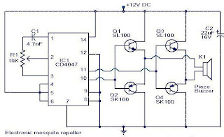
ELECTRONIC MOSQUITO REPELLER

  1. Here is the circuit diagram of an ultrasonic mosquito repeller.
  2. The circuit is based on the theory that insects like mosquito can be repelled by using sound frequencies in the ultrasonic (above 20KHz) range.
  3. The circuit is nothing but a PLL IC CMOS 4047 wired as an oscillator working at 22KHz.
  4. A complementary symmetry amplifier consisting of four transistor is used to amplify the sound.
  5. The piezo buzzer converts the output of amplifier to ultrasonic sound that can be heard by the insects.


    NOTES:
    • Assemble the circuit on a general purpose PCB.
    • The circuit can be powered from 12V DC.
    • The buzzer can be any general purpose piezo buzzer.
    • The IC1 must be mounted on a holder.

Wednesday, October 12, 2011

SIMPLE SOUND GENERATOR CIRCUIT

  1. This is a real scream generator circuit suitable for any purpose like alarm or car horn.
  2.  The circuit is based on two transistors Q1 and Q2.
  3. When you press the switch S2 the siren starts up moving to a high frequency.
  4. When the switch is released the tone slips down until you shift it up again by pushing the switch S2.


   NOTES:
  • Adjustment of tone quality can be obtained by different values for C2.
  • If the alarm oscillates before S2 is pressed.The transistor is leaky, replace it.
  • S1 can be used as a power switch.