- A high quality stereo FM transmitter circuit is shown here. The circuit is based on the IC BA1404 from ROHM Semiconductors.
- BA1404 is a monolithic FM stereo modulator that has built in stereo modulator, FM modulator, RF amplifier circuitries. The FM modulator can be operated from 76 to 108MHz and power supply for the circuit can be anything between 1.25 to 3 volts.
- In the circuit R7, C16, C14 and R6, C15, C13 forms the pre-emphasis network for the right and left channels respectively.
- This is done for matching the frequency response of the FM transmitter with the FM receiver. Inductor L1 and capacitor C5 is used to set the oscillator frequency.
- Network C9,C10, R4,R5 improves the channel separation. 38kHz crystal X1 is connected between pins 5 and 6 of the IC.
- Composite stereo signal is created by the stereo modulator circuit using the 38kHz quartz controlled frequency.
Thursday, February 17, 2011
STEREO FM TRANSMITTR CIRCUIT USING BA1404
Tuesday, February 15, 2011
BUCK BOOST CONVERTER CIRCUIT
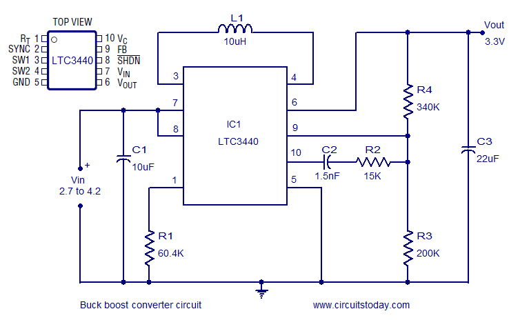
- A very efficient buck boost converter circuit is shown here. The circuit is based on the LTC3440 buck boost regulator IC from Linear Technology.
- The LTC3440 requires only one inductor and provides up to 96% efficiency. There is no need of Schottky diode for applications where output voltage is less than 4.3V and the IC can deliver up to 600mA output current.
- In the circuit the IC is wired as a buck boost regulator providing 3.3V output from a 2.7 to 4.2V input.
- R1 is the timing resistor which determines the oscillator frequency and it can be varied between 300 KHz to 2MHz by varying the value of R1. C1 is the input bypass capacitor for reducing noise and C3 is the output filter capacitor.
Thursday, February 3, 2011
AM RECEIVER USING ZM 414Z

- This is the circuit diagram of the simplest single chip AM radio
- The circuit is designed around the IC ZN414Z which is a ten transistor tuned radio frequency receiver .The IC has only three leads and is available in the TO92 package.
- All necessary circuits required for an AM receiver (RF amplifier, detector and AGC are incorporated inside the IC).
- Capacitor C4 decouples DC from the output of the IC and C1 bye-passes the noise.
- Transistor Q1 and associated components forms a classic driver stage for the headphone.
- Head phone is connected across the resistor R5 and R4 gives necessary biasing for the transistor Q1.
Wednesday, February 2, 2011
AUTOMOBILE TURN SIGNAL CIRCUIT
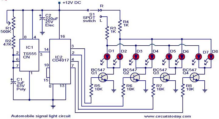
- This is a simple circuit that can be used as a sequencial signal light in automobiles.
- The circuit is based on two ICs. A TS 555 CN CMOS timer IC and a CD4017 decade counter IC
- The IC1 is wired as an astable multivibrator to trigger the counter IC. When triggered, the outputs of the IC 2 (pins 3, 2, 4 and 7) will go high and low in sequence and the speed of this sequencing will be proportional to the triggering frequency.
- The transistors Q1 to Q4 drives the corresponding LEDs.
- The switch S1 can be used to select the direction of turning and the LEDs arranged at the corresponding side of vehicle will start sequencing.
Tuesday, February 1, 2011
FAN SPEED CONTROLLER USING LM2941
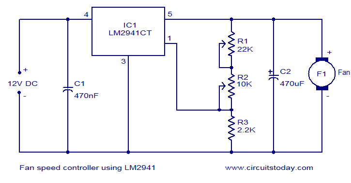
- Many electronic circuits related to fan speed controlling have been published here and this one is just another approach.
- The circuit diagram shown here is of 12V DC fan speed controller using the IC LM2941CT which is a low drop out 1A voltage regulator. The IC has a dropout voltage as low as 0.5 and has also many useful features like power supply reverse protection, thermal protection, short circuit protection etc.
- The maximum output current the IC can source is 1A.
- The 12V DC supply is connected between the Vin (pin4) and ground (pin3) of the IC.
- The load, which is the fan, is connected across the Vout (pin5) and ground (pin3) of the IC. The network comprising of potentiometers R1, R2 and resistor determines adjust current (Iadj) of the IC.
Sunday, October 3, 2010
TWEETER CROSSOVER CIRCUIT

- A single coil speaker is not good in handling high and low frequency at the same time.
- If we could filter out the low frequency and play it through a tweeter ,it will produce more sound quality than using a single speaker.
- This is what is realized here.
Monday, September 20, 2010

Wednesday, September 15, 2010

Monday, September 6, 2010
10V SWITCHING REGULATOR USING LM5007

- The circuit diagram shown here is of a 10V switching regulator based on the LM5007 from National Semiconductors.
- The LM5007 is an integrated step down switching regulator which has all necessary systems required for making a cost effective and reliable switching regulator circuit.
- The IC is available in MSOP-8, LLp-8 packages and has a lot of built in features like thermal shut down, under voltage lock out, duty cycle limiting, current limiting etc.
- The output voltage of this regulator can be adjusted using the resistor R3 and R4.
- OR the given values of R3 and R4 in the circuit diagram, the output voltage will be 10V.
- he equation governing the output voltage is Vout = 2.5 x (R3+R4)/R4. Resistor R1 sets the switch on time and C4 is the boost boot strap capacitor.
- Resistor R2 determines the variation of OFF time and C3 is a decoupling capacitor.
NOTES:
- The supply voltage can be anything between 12 to 72V DC.
- Output voltage can be adjusted using R3 and R4.
- C1 and C5 are polyester capacitors.
- C1 and C2 must be rated at least 100V.
- R5 and C5 forms a filter network.
- The output current limit of LM5007 is 700mA.
Tuesday, August 17, 2010
3 INPUT MICROPHONE PREAMPLIFIRE

- The circuit given here is of a three input mic mixer cum preamplifier using the IC LM348. The LM348 is a high gain, internally compensated quad operational amplifier with a class AB output stage.
- The IC has very low input supply current drain (0.6mA/ opamp) and operates from a dual power supply.
- The output of these three amplifiers are tied together and connected to the inverting input of the IC1a which is wired as an inverting amplifier.IC1a mixes the signals from each channel and also works as the output stage.
Tuesday, August 10, 2010
STEREO PREAMPLIFIER WITH TONE CONTROL

- Here is the circuit diagram of an excellent stereo preamplifier with tone control using the IC TDA1524 from Phillips.
- The IC requires very few external components, has very low noise and has a wide power supply voltage range.
- POTs R1 to R4 can be used for controlling the volume, balance, bass and treble respectively.
Wednesday, August 4, 2010
DARK DETECTOR

- The dark detector circuit shown here can be used to produce an audible alarm when the light inside a room goes OFF.
- The circuit is build around timer IC NE555.A general purpose LDR is used for sensing the light.
- When proper light is falling on the LDR its resistance is very low.
- When there is no light the LDR resistance increases.
- At this time the IC is triggered and drives the buzzer to produce an alarm sound.
- If a transistor and relay is connected at the output (pin3) of IC1 instead of the buzzer, electrical appliances can be switched according to the light.
Tuesday, August 3, 2010
PARKING SENSOR CIRCUIT


- This simple circuit can be used as an aid for sensing the distance between the rear bumper of the car and any obstacle behind the car. The distance can be understood from the combination of the LEDs (D5 to D7) glowing. At 25cm D7 will glow, at 20 cm D7&D6 will glow and at 5cm D7, D6 and D5 will glow. When the obstacle is beyond 25 cm none of the above LEDs will glow.
- Two ICs are used in the circuit. The IC1 (NE555) is wired as an astable multivibrator for driving the IR Diode D1 to emit IR pulses. The operating frequency of the transmitter is set to be 120Hz.
- The IR pulses transmitted by D1 will be reflected by the obstacle and received by the D2 (IR photo diode).The received signal will be amplified by IC2a.The peak of the amplified signal will be detected by the diode D4 and capacitor C4.R5 and R6 compensates the forward voltage drop of D4.The output voltage of the peak detector will be proportional to the distance between car’s bumper and obstacle.
Saturday, July 31, 2010
100 WATT INVERTER CIRCUIT

- Here is a 100 Watt inverter circuit using minimum number of components.I think it is quite difficult to make a decent one like this with further less components.Here we use CD 4047 IC from Texas Instruments for generating the 100 Hz pulses and four 2N3055 transistors for driving the load
- These pulse trains are preamplifed by the two TIP122 transistors.The out puts of the TIP 122 transistors are amplified by four 2N 3055 transistors (two transistors for each half cycle) to drive the inverter transformer.
- The 220V AC will be available at the secondary of the transformer.Nothing complex just the elementary inverter principle and the circuit works great for small loads like a few bulbs or fans.If you need just a low cost inverter in the region of 100 W,then this is the best.
NOTES:
- A 12 V car battery can be used as the 12V source.
- Use the POT R1 to set the output frequency to50Hz.
- For the transformer get a 9-0-9 V , 10A step down transformer.But here the 9-0-9 V winding will be the primary and 220V winding will be the secondary.
- If you could not get a 10A rated transformer , don’t worry a 5A one will be just enough. But the allowed out put power will be reduced to 60W.
- Use a 10 A fuse in series with the battery as shown in circuit.
- Mount the IC on an IC holder.
- Remember,this circuit is nothing when compared to advanced PWM inverters.This is a low cost circuit meant for low scale applications.
Thursday, July 29, 2010
TELEPHONE IN USE INDICATOR

- Here is a simple circuit that can be used as a telephone status indicator. When the telephone is in use (off hook) the transistor Q1 switches ON making the red LED D2 glow.
- When the telephone is not in use (on hook) the Q1 turns OFF and Q2 turns ON.
- This makes the red LED D2 off and green LED D3 ON.
Monday, July 26, 2010
AIR CRAFT WARNING LIGHT CIRCUIT
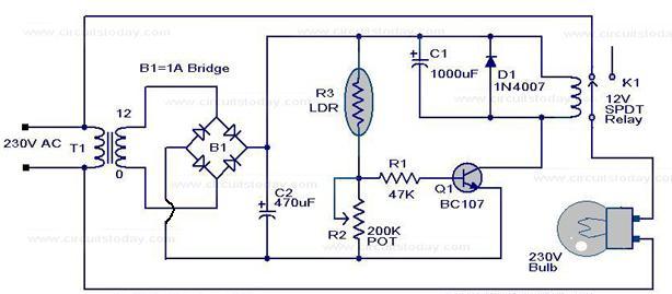
- Here is low cost circuit that can be used for implementing a warning light on the top of tall structures as a warning for low flying aircrafts.
- Usually such lights are just stay glow type .Here our light is a flashing type, and surely this will draw more attention and of course add more safety.
- When the AC mains is switched on the bulb will get supply and it will glow.
- When the bulb glows the LDR adjacent to it gets illuminated and it’s resistance drops.This will increase the voltage drop at the base of transistor Q1 and it goes on.When Q1 is on the relay is activated and trips the contacts to make the bulb off.Now the LDR resistance increases and the voltage drop across base of Q1 decreases to make it off.
- The relay will be de-energized and the bulb glows.This cycle repeats to produce a continuous flashing of the bulb.
- Since the capacitor C1 is connected across the relay the relay will remain activated for some more time even after the transistor Q1 is OFF,making the bulb to stay off for some more time.
NOTES:
- The LDR should be mounted at some place near to the bulb so that when bulb glows the light falls on the LDR.
- Set up the circuit as said above and power up.Then adjust the POT R2 so that the bulb starts flashing.Done!The circuit is ready.
- Some parts of the circuit are live with potential shock hazard.Be careful!.
- Bulb of any Watts can be used as load provided that a relay with suitable power rating is used.
- All capacitors are electrolytic and must be rated 25Volts.
Friday, July 23, 2010
BATTERY ELIMINATOR CIRCUITS

- Here is the circuit diagram of a battery eliminator circuit that can be used as a replacement for 9V PP3 batteries.
- The circuit given here can be used to power any device that operates from a 9V battery.
- The transformer T1 steps down the mains voltage and bridge D1 performs the job of rectification.
- Capacitor C1 is a filter. IC LM317T is the regulator here.
- The value of R1, R2 and R3 are so selected that the output voltage of IC1 will be steady 9 volts.
NOTES:
- Assemble the circuit on a good quality PCB.
- Transformer T1 can be a 230V primary, 9V secondary, 1.5A step down transformer.
- If 1A Bridge is not available, then make one using four 1N 4007 diodes.
- Do not connect loads that consume more than 1.5A to this circuit.
- A heat sink is recommended for IC1.
Friday, July 16, 2010
CONTECT LESS TELEPHONE RINGER CIRCUIT

- The contact less telephone ringer circuit can produce a ring as well as a visual indication when a call comes.
- The main advantage is that since there is no direct contact between the phone line and the circuit there is no chance for a loading or disturbance in the telephone line.
- When the telephone rings 60 Hz AC signal is generated which produces a proportional magnetic field around the telephone lines.
- These magnetic field will be picked up by the coil L1 due to electromagnetic induction.
- A proportional voltage is developed across L1 and it will bias transistor Q1 to ON.
- This results in the conduction of transistors Q2,Q3 andQ4.The buzzer will ring and the LED will glow.
Thursday, July 15, 2010
VHF FIELD STRENGTH METER

- This is a simple and low cost wide band VHF field strength meter.
- The field strength is measured by converting the radio signal to DC and measuring it.
- The RF signal will be picked up by the coil and rectified by the diode D1.Even a very small DC voltage is sufficient to alter the biasing of FET and it will be reflected in the meter as an indication of the presence of a radio signal.
- he meter can be calibrated by adjusting the preset R2 to make meter M1 read ZERO in the absence of any radio signal.
- This circuit is not very sensitive, but can sense radio signals from hand held FM transmitters up to a distance of few meters( ideal for theoretical demonstrations).
NOTES:
- The circuit can be assembled on a general purpose PCB.
- Use a 9V PP3 battery for powering the circuit.
- Use a 250uA FSD current meter for M1.Using a lower FSD meter will improve sensitivity.
- The coil L1 can be made by making 6 turns of 20 SWG enameled copper wire on a ¼ inch plastic former.
- The antenna can be a telescopic whip antenna.
Wednesday, April 21, 2010
SELECTIVE TIMER ALARM

- A timer circuit using IC 4060 is given here. The IC 4060 is a 14 stage binary counter with a built-in oscillator.
- R2, R7, C1 are the components that determine the frequency of the oscillator and the outputs will become high one after other and only one at a time.
- The last five outputs are only used here. The high pulses from the outputs are used to trigger the NE555 IC.
- Here NE555 is wired as a monostable multivibrator. The buzzer will produce the alarm when the output of IC2 goes high.
- The duration of the alarm depends on the components C3 and R5.The duration can be adjusted by varying the value of C3.
- The alarm will automatically turn OFF after the predetermined time. The trigger pin of IC2 will be normally positive.
- When the Q1 is forward biased by the positive pulse at its base from IC1, the capacitor C2 becomes charged and reduces the voltage at trigger pin of IC2.This triggers the IC.When the capacitor is fully charged the pin 2 becomes again positive.
- The maximum duration from timer IC 4060 will be at pin 3. The times decrease by half in the pins 2, 3, 15, and 13 respectively. The timer duration can be varied by varying the capacitor C1.
NOTES:
- Use 6V DC for powering the circuit.
- Assemble the circuit on a good quality PCB.
- Mount the ICs on holders.
- The switch S2 can be a single pole five throw rotary switch.
- The switch S1 can be a push button switch.
- S1 is used to reset the timer.
- S2 is used to select the alarm time.
- R7 can be used for the fine adjustment of alarm time.
Subscribe to:
Posts (Atom)