rajkot

Wednesday, April 21, 2010

SELECTIVE TIMER ALARM

  1.  A timer circuit using IC 4060 is given here. The IC 4060 is a 14 stage binary counter with a built-in oscillator.
  2. R2, R7, C1 are the components that determine the frequency of the oscillator and the outputs will become high one after other and only one at a time.
  3.  The last five outputs are only used here. The high pulses from the outputs are used to trigger the NE555 IC.
  4.  Here NE555 is wired as a monostable multivibrator. The buzzer will produce the alarm when the output of IC2 goes high.
  5.  The duration of the alarm depends on the components C3 and R5.The duration can be adjusted by varying the value of C3.
  6.  The alarm will automatically turn OFF after the predetermined time. The trigger pin of IC2 will be normally positive.
  7.  When the Q1 is forward biased by the positive pulse at its base from IC1, the capacitor C2 becomes charged and reduces the voltage at trigger pin of IC2.This triggers the IC.When the capacitor is fully charged the pin 2 becomes again positive.
  8.  The maximum duration from timer IC 4060 will be at pin 3. The times decrease by half in the pins 2, 3, 15, and 13 respectively. The timer duration can be varied by varying the capacitor C1.


       NOTES:
  • Use 6V DC for powering the circuit.
  • Assemble the circuit on a good quality PCB.
  • Mount the ICs on holders.
  • The switch S2 can be a single pole five throw rotary switch.
  • The switch S1 can be a push button switch.
  • S1 is used to reset the timer.
  • S2 is used to select the alarm time.
  • R7 can be used for the fine adjustment of alarm time.

Tuesday, April 20, 2010

SIGNAL TRACER CIRCUIT

  1. A high gain amplifier circuit that can be operated from a battery pack of 6 or 9 volt battery pack is shown here.
  2. The IC1 uA 741 is wired as a high gain non-inverting amplifier and its output is amplified by a pair of complementary transistors (Q1 & Q2) to drive the speaker.The negative feedback from the common emitter junction of the two transistor stabilizes the gain of the circuit.
  3. The resulting audio output is sufficient to serve as a signal tracer. 

       NOTES:
  • Assemble the circuit on a  good quality PCB or  common board .
  • The POT R6 can be used as a volume controller.
  • The circuit can be powered from a 6 or 9V DC battery pack.
  • The IC1 must be mounted an an IC base.
  • All capacitors must be rated at least 15V.

Monday, April 19, 2010

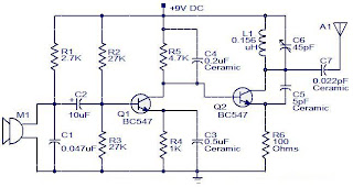
MIDIUM POWER FM TRANSMITTER CIRCUIT

  1. This is the circuit diagram of a moderate power FM transmitter circuit employing two transistors.The voice signals picked by the microphone will be amplified by the transistor Q1.
  2.  The second transistor is wired as an oscillator operating in the FM band.
  3.  The output of T1 is given to the base of T2.T2 performs the modulation also.
  4.  The tank circuit comprising of components L1 and C6 determines the frequency of the signal, and can be varied by adjusting C6.The capacitor C7 couples the FM signal to the antenna.


        NOTES:
  • You can assemble the circuit on a general purpose PCB.
  • The circuit can be powered from a9V PP3 battery.
  • The Antenna A1 can be a 1M long wire.
  • The inductor L1 can be made by making 6 turns of 0.8mm enameled copper wire on a 5.5mm diameter/4.5mm length plastic former.
  • With a matching antenna and proper tuning this transmitter can have range upto 100meters.


Sunday, April 18, 2010

SIMPLEST FM TRANSMITTER

  1. Here is the circuit diagram of the simplest FM transmitter using a transistor.
  2. Great performance or range is not guarenteed here, because this is an elementary design.
  3. General purpose radio frequency transistor BF 494 (Q1) is used here for obtaining FM modulation.
  4. A condenser mic is used here to pickup the sound.
  5. The condenser mic converts the sound to electrical variations and this variations are fed to the base of Q1 , which performs the amplification as well as modulation.
  6. The capacitor  C2   and L1 determines the frequency of transmission.The circuit can be powered from a 9V transistor radio battery.
 

      NOTES:
  • The coil L1 can be made by winding 8 turns of 1mm thick enamel coated copper wire on a ball pen refill.  The coil should be tapped  at the  center for connecting the antenna.
  • A 30 cm wire can be used as an antenna.
  • Remember! This circuit is an elementary circuit.No good performance or range is not guaranteed.Ideal for demo applications only.I got only 8 meter range with some decent sound quality.
  • Battery is strictly recommended because mains powered supply may induce additional noise.

Thursday, April 15, 2010

RADIO COLLAR TRANSMITTER

  1. This is the circuit diagram of a radio transmitter suitable for fitting on radio collars.
  2. The circuit transmits a pulse in the FM between band 88MHz to 105Mhz , which can be adjusted.
  3. IC Ne 555 is wired as an astable multivibrator for producing the tone.L1 ,C3 and Q1 forms the modulator.
  4. Q2 performs the final power amplification. 
  5. For the inductor make 5 turns of .5 mm dia insulated copper wire on a standard ball pen refill.
  6. Remove the refill and make a tap at the center of coil.


  7.  


Monday, April 12, 2010

SPEECH AMPLIFIER CIRCUIT

  1. This circuit given here can be housed in the box containing the speaker to form a handy microphone amplifier.
  2. The device can be used by teachers,guides,lecturers etc for speaking in a crowdy or noisy environment.
  3.  The circuit is designed base on the audio power amplifier IC TDA 7052.
  4.  The IC can deliver a maximum power output of 1.2 W at a 6V supply.
  5. The audio signal from the microphone is pre amplified by the amplifier based on Q1 (BC 547) and give to the input of IC1 (pin 2).
  6.  The POTR5  acts as a volume control.
  7.  The capacitor C3 is used to bye pass the upper frequencies in order to avoid the Larsen’s effect(the microphone picking up speaker output to cause howls).

Sunday, April 11, 2010

HI-FI DX BASS CIRCUIT

  1. The circuit that designed is a passive one but you can make it an active one by adding a pre amp at the output.
  2. The first stage acts as a main tone stage. It balances the bass and the treble. The 0.01 cap is for high frequency while the 0.22uF cap is for low frequency.
  3.  The second stage is for sound compression.
  4.  he caps works the same as at the first stage only that they are there to start the sound compression that is received from the input stage.
  5.  The 2.2k resistor delays the sound thereby multiplying the compression.
  6.  The 10k variable resistor is there used to tune the compression depending on the frequency of the speaker. If you are using 4 to 6 inches hi-fi speakers, I advise you to keep the 10k variable resistor at 0 ohm.
  7. The circuit is not copyrighted and you can change it to suit your requirement. All I ask is to be posting the updates of the circuit design on the site. 

Wednesday, April 7, 2010

FM TRACKING TRANSMITTER

  1. The circuit presented her will transmit a audio tone in the FM  band.
  2. The circuit can be used as a tracking signal transmitter or a remote control transmitter.
  3. The circuit uses only easily available components and any one can build this.The transmitter has a range of 100m @ 9V supply, with a matching antenna.
  4. The NE555 timer (IC1) is used for producing the audio tone.
  5. The first JFET(Q1) is wired as a Hartley oscillator which is frequency modulated by the audio tone.The second(Q2) JFET is wired as a buffer to isolate the oscillator based on Q1 from the antenna.
  6. The diode D1 is used as a varactor here.The diode is reverse biased by the ramping voltage produced at the pin 6&2 of the IC1.
  7. This results in the change of junction capacitance of reverse biased diode , which in turn alters the frequency of the oscillator to attain the frequency modulation.


          NOTES:
  • The inductor L1 can be made by winding 5 turns of  18 SWG enameled copper wire on a 3/8 inch long, 3/16 inch diameter plastic tube .The coil must be tapped at the center.
  • The antenna can be a 20cm long wire.
  • The circuit can be powered from a 9V battery.
  • POT R6 can be used to adjust the transmission power.

Tuesday, April 6, 2010

INFRARED MOTION DETECTOR CIRCUIT

  1. Here is the circuit diagram of an infrared motion detector that can be used to sense intrusions.
  2. Infra red rays reflected from a static object will be in one phase, and the rays reflected from a moving object will  be in another phase.
  3. The circuit uses this principle to sense the motion.
  4. The IC1 (NE 555)  is wired as an astable multivibrator .
  5. The IR diode connected at the output of this IC produces infrared beams of frequency 5Khz.These beams are picked by the photo transistor Q1.
  6. At normal condition ie; when there is no intrusion the output pin (7) of IC2 will be low.
  7. When there is an intrusion the phase of the reflected waveforms has a difference in phase and this phase difference will be picked by the IC2.
  8. Now the pin 7 of the IC 2 goes high to indicate the intrusion.An LED or a buzzer can be connected at the output of the IC to indicate the intrusion.


         NOTES:
  • Comparators IC2a and IC2b are belonging to the same IC2  (LM1458).So the power supply is shown connected only once.No problem.
  • When there is disturbance in the air or vehicles passing nearby,the circuit may get false triggered.
  • POT R5 can be used for sensitivity adjustment.

Monday, April 5, 2010

REMOTE CONTROLLED APPLIANCE SWITCH

  1. Here is a versatile remote controlled appliance switch that can ON or OFF any appliance connected to it using a TV remote.
  2. IR remote sensor IC TSOP 1738 is used for receiving the signal.
  3.   Normally when no signal is falling on IC3 the output of it will be high.
  4. This makes Q1 OFF.When a signal of 38 KHz from the TV remote falls on the IC3 its output goes low.
  5.  This makes Q1 conduct and a negative pulse is obtained at pin 2 of IC 1 NE 555.
  6.  Due to this IC1 wired as a monostable multivibrator produces a 4 Sec long high signal at its out put.
  7.  This high out put is the clock for IC 2 which is wired as a Flipflop and of , its two outputs pin 3goes low and pin 2 goes high.
  8. The high output at pin 2 is amplified to drive the relay .For the next signal the outputs of IC2 toggles state.
  9.   Result, we get a relay toggling on each press on the remote.Any appliance connected to this circuit can be switched ON or OFF.


          NOTES:
  •  Before wiring the circuit make sure that the carrier frequency of theTV remote you have is 38 kHz.For that wire the sensor part only ,point yourremote to the TSOP1738 and press any switch.If out put of TSOP1738 goeslow then OK, your remote is of 38Khz type.Nothing to worry almost all TVremote are of this type.
  •   You can use any switch  of the remote because for any switch the code only changes,the carrier frequency remains same.We need this carrier frequency only.
  •   Assemble the circuit on a good quality PCB or common board.
  •  The appliance can be connected through NO or NC and C contacts of the relay .
  • Use a regulated 6V power supply for the circuit.

Saturday, April 3, 2010

ELECTRONICS TOSS CIRCUIT

  1. The circuit given here can be used for tossing head or tail.
  2. There are many games in which a tossing is required to start and this circuit can be used in all such instances.
  3.  The circuit uses two ICs NE 555 timer (IC1) and 74LS76 dual JK flip flop (IC2).The IC 1 is wired as an astable multi vibrator operating at 10Hz.
  4.  The output of IC1 is inverted by using the transistor Q1.
  5.  The collector of Q1 is connected to the pin 1 of IC2 via the push button switch S1.
  6.  The IC2 is wired in toggle mode.
  7.  When push button S1 is pressed the output pins 14 and 15 of IC2 starts toggling in state.
  8.  The LEDs connected to these pins also toggles (Since the frequency of toggling is 10Hz, we feel both LEDs glowing).
  9. When push button S1 is released either one of the LED remains ON indicating the head or tail.


        NOTES:
  • The circuit can be powered from 5 V DC.
  • Switch S1 is a push button switch.
  • The ICs must be mounted on holders.
  • The circuit can be assembled on a general purpose PCB.

Friday, April 2, 2010

MINIATURE FM TRANSMITTER

  1. This could be the simplest FM transmitter circuit you can find on the internet.
  2. Only using a single transistor and few passive components, this transmitter can deliver signals up to 50 meters. 
  3.  The transistor Q1 serves as the modulator as well as oscillator.
  4. Capacitor C2 and inductor L1 forms the necessary tank circuit for making oscillation.
  5.  The voice to be transmitted is coupled to the base of Q1 using an electret microphone.
  6. The FM signal available at the collector of Q1 is radiated using the antenna.