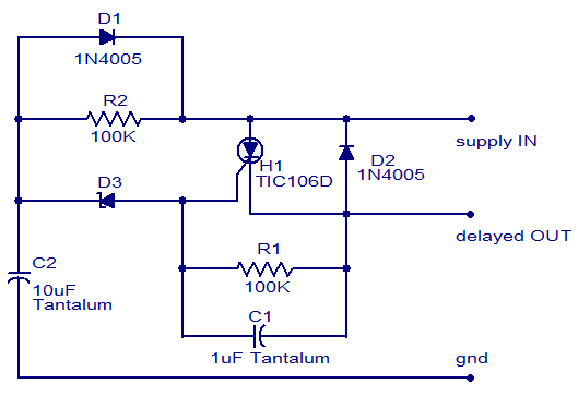
- The circuit diagram shown here is of a simple DC power delay circuit that is based on an SCR.
- This circuit is a very handy one and can be employed in many applications.
- When the input power is applied the capacitor C2 charges through resistor R2 and when the voltage across the capacitor just exceeds the Zener diode D3’s breakdown voltage, it breaks down and the SCR H1 is triggered and the delayed power will be available at the delayed OUT terminal.
NOTES:
- The circuit must be assembled on a good quality PCB.
- The Zener diode must be rated half the input supply voltage.
- The current capacity of the circuit depends on the SCR and here it is 4A.