- A high quality stereo FM transmitter circuit is shown here. The circuit is based on the IC BA1404 from ROHM Semiconductors.
- BA1404 is a monolithic FM stereo modulator that has built in stereo modulator, FM modulator, RF amplifier circuitries. The FM modulator can be operated from 76 to 108MHz and power supply for the circuit can be anything between 1.25 to 3 volts.
- In the circuit R7, C16, C14 and R6, C15, C13 forms the pre-emphasis network for the right and left channels respectively.
- This is done for matching the frequency response of the FM transmitter with the FM receiver. Inductor L1 and capacitor C5 is used to set the oscillator frequency.
- Network C9,C10, R4,R5 improves the channel separation. 38kHz crystal X1 is connected between pins 5 and 6 of the IC.
- Composite stereo signal is created by the stereo modulator circuit using the 38kHz quartz controlled frequency.
Thursday, February 17, 2011
STEREO FM TRANSMITTR CIRCUIT USING BA1404
Tuesday, February 15, 2011
BUCK BOOST CONVERTER CIRCUIT
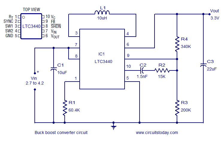
- A very efficient buck boost converter circuit is shown here. The circuit is based on the LTC3440 buck boost regulator IC from Linear Technology.
- The LTC3440 requires only one inductor and provides up to 96% efficiency. There is no need of Schottky diode for applications where output voltage is less than 4.3V and the IC can deliver up to 600mA output current.
- In the circuit the IC is wired as a buck boost regulator providing 3.3V output from a 2.7 to 4.2V input.
- R1 is the timing resistor which determines the oscillator frequency and it can be varied between 300 KHz to 2MHz by varying the value of R1. C1 is the input bypass capacitor for reducing noise and C3 is the output filter capacitor.
Thursday, February 3, 2011
AM RECEIVER USING ZM 414Z

- This is the circuit diagram of the simplest single chip AM radio
- The circuit is designed around the IC ZN414Z which is a ten transistor tuned radio frequency receiver .The IC has only three leads and is available in the TO92 package.
- All necessary circuits required for an AM receiver (RF amplifier, detector and AGC are incorporated inside the IC).
- Capacitor C4 decouples DC from the output of the IC and C1 bye-passes the noise.
- Transistor Q1 and associated components forms a classic driver stage for the headphone.
- Head phone is connected across the resistor R5 and R4 gives necessary biasing for the transistor Q1.
Wednesday, February 2, 2011
AUTOMOBILE TURN SIGNAL CIRCUIT
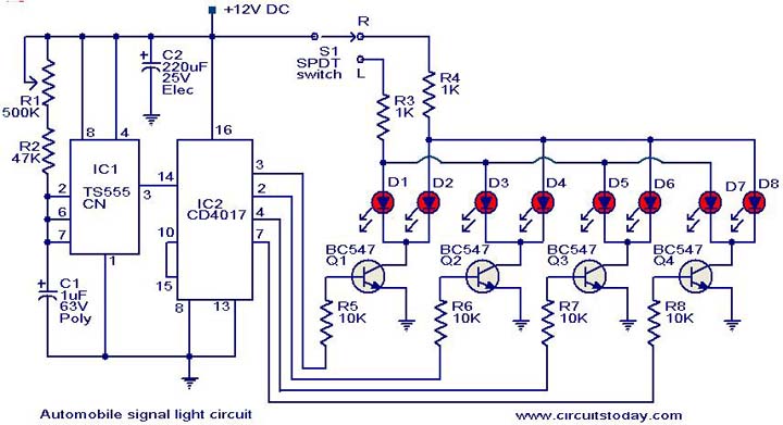
- This is a simple circuit that can be used as a sequencial signal light in automobiles.
- The circuit is based on two ICs. A TS 555 CN CMOS timer IC and a CD4017 decade counter IC
- The IC1 is wired as an astable multivibrator to trigger the counter IC. When triggered, the outputs of the IC 2 (pins 3, 2, 4 and 7) will go high and low in sequence and the speed of this sequencing will be proportional to the triggering frequency.
- The transistors Q1 to Q4 drives the corresponding LEDs.
- The switch S1 can be used to select the direction of turning and the LEDs arranged at the corresponding side of vehicle will start sequencing.
Tuesday, February 1, 2011
FAN SPEED CONTROLLER USING LM2941
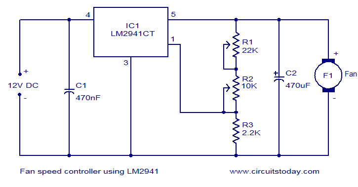
- Many electronic circuits related to fan speed controlling have been published here and this one is just another approach.
- The circuit diagram shown here is of 12V DC fan speed controller using the IC LM2941CT which is a low drop out 1A voltage regulator. The IC has a dropout voltage as low as 0.5 and has also many useful features like power supply reverse protection, thermal protection, short circuit protection etc.
- The maximum output current the IC can source is 1A.
- The 12V DC supply is connected between the Vin (pin4) and ground (pin3) of the IC.
- The load, which is the fan, is connected across the Vout (pin5) and ground (pin3) of the IC. The network comprising of potentiometers R1, R2 and resistor determines adjust current (Iadj) of the IC.
Subscribe to:
Posts (Atom)