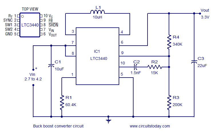
- A very efficient buck boost converter circuit is shown here. The circuit is based on the LTC3440 buck boost regulator IC from Linear Technology.
- The LTC3440 requires only one inductor and provides up to 96% efficiency. There is no need of Schottky diode for applications where output voltage is less than 4.3V and the IC can deliver up to 600mA output current.
- In the circuit the IC is wired as a buck boost regulator providing 3.3V output from a 2.7 to 4.2V input.
- R1 is the timing resistor which determines the oscillator frequency and it can be varied between 300 KHz to 2MHz by varying the value of R1. C1 is the input bypass capacitor for reducing noise and C3 is the output filter capacitor.